You may have heard the use of High Bandwidth Memory (HBM) on most of AMD’s new graphics cards. However, what exactly does it do and how it differs from traditional GDDR memory? Let’s find out.
In June 2015, AMD launched the Radeon R9 Fury X, Fury and Nano to the public, which is the first series of graphics cards utilizing HBM in the industry. NVIDIA continued to use GDDR5 and GDDR5X memory on the consumer cards, but released the Tesla P100 workstation card with HBM2 in April 2016.
Working Principle
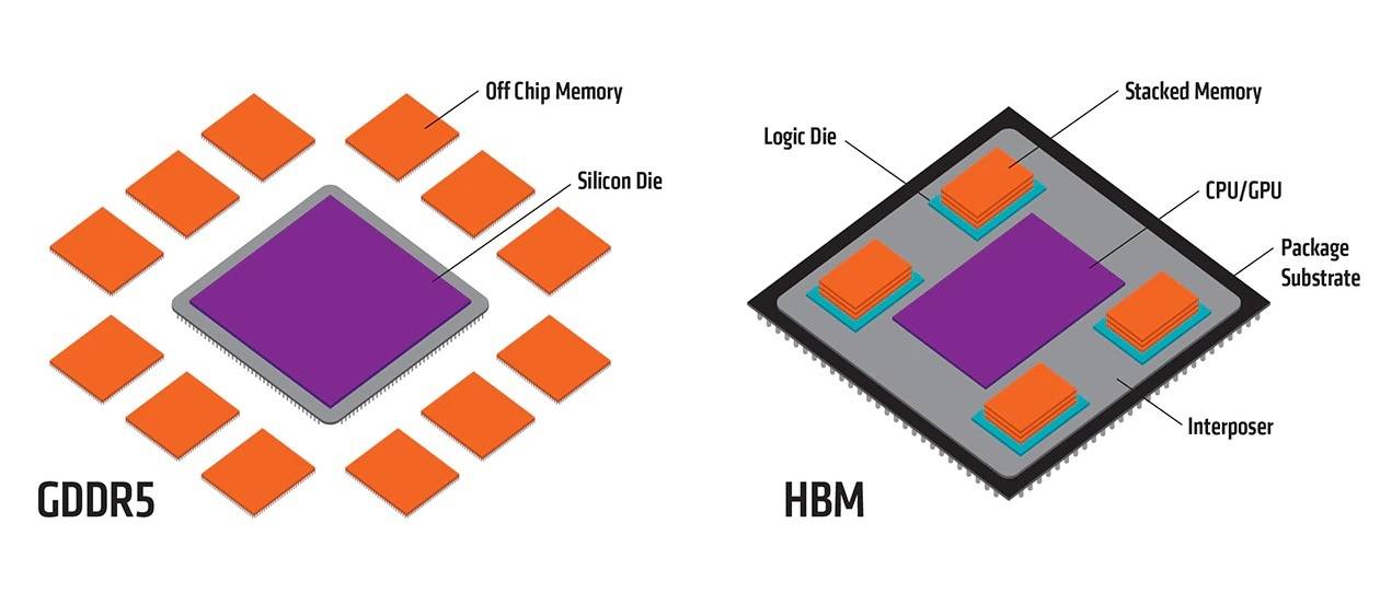
Physically, standard GDDR memory chips are soldered to the printed circuit board (PCB) around the GPU die. HBM chips, on the other hand, are installed on top of the package substrate right next to the GPU die.
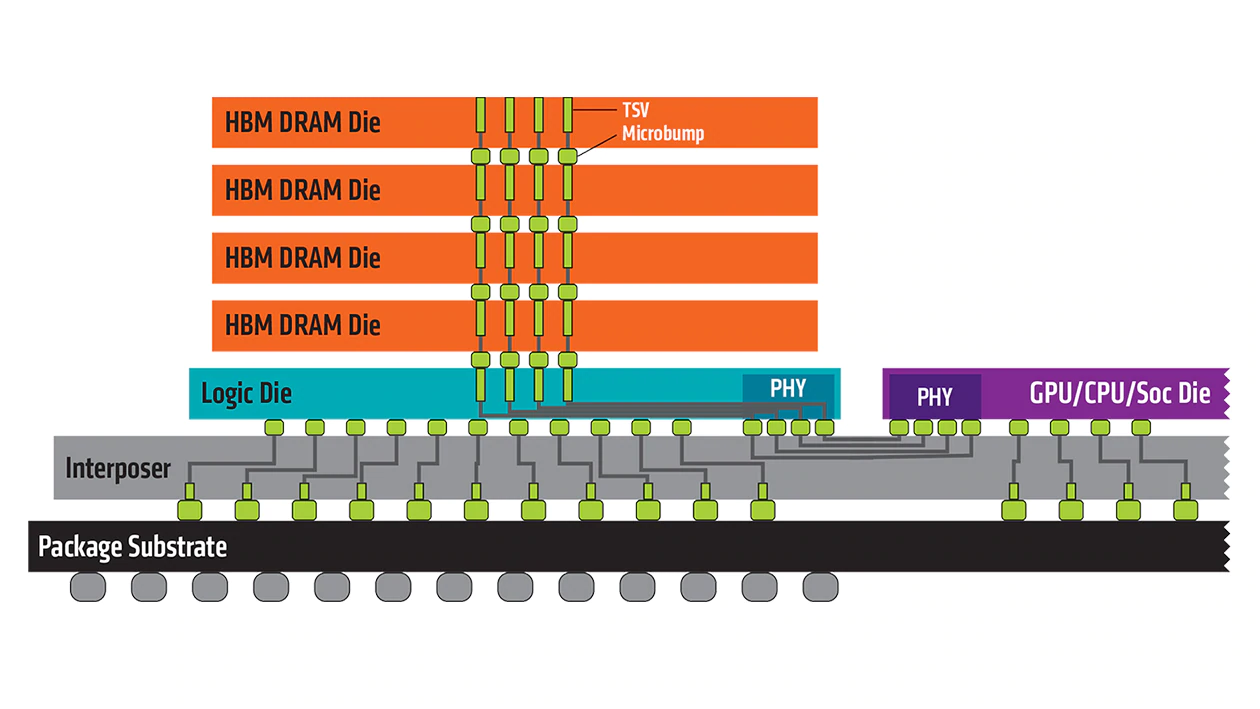
HBM modules, including the memory controller, can be stacked vertically to further reduce footprint. Memory chips are interconnected by through-silicon via (TSV) and communicate with the GPU through the Interposer layer.
HBM allows a maximum eight DRAM dies per stack, which has a transfer rate of up to 2 GT/s (HBM 2). Each HBM DRAM die has two 128-bit channel, compared to GDDR5’s single 32-bit channel. Therefore, a HBM stack of four dies can have an extremely wide memory bus at 1024-bit and over 100 GB/s of total bandwidth.
Advantage
Due to the HBM modules are soldered so close to the GPU die physically, you get the benefit of shorter paths for data transmission. Combined with the super wide memory bus, the GPU can be fed with information very responsively (lower latency), while consumes considerably less power to achieve similar bandwidth than GDDR5 memory.
The capability of stacking memory chips vertically and on the same substrate as the GPU die allows manufacturers to save precious space on the PCB. Higher-end graphics card can now be made smaller without sacrificing performance.
Disadvantage
Despite the aforementioned pros for switching to HBM, GDDR5 and GDDR6 memory remain to be the industry standard for consumer graphics cards. The complicated manufacturing processes for stacking multiple chips on top of each other drive the production cost and time high.
Normal users can hardly notice the difference with HBM and GDDR5 memory for gaming. And the introduction of GDDR6 memory with higher bandwidth and lower power consumption makes the incentives of switching to HBM smaller.
Feel free to leave comments below, if you have any opinion about this website. Share the website around if you enjoy reading it. Subscribe to our Newsletter or follow our Google+, Facebook and Twitter.
Support this website simply by shopping in Amazon. It will give us small kickbacks, if you use the above affiliate links to make any purchases, which will help us grow.






I invented the 3D stacked “phased SRAM” at Cypress Semiconductor ~2002. I submotted a patent but the Specialty Memory Dividion was shut down. I was designing 4 chip memory board “leap-frogers” that produced the next rev of memory on the release of any new rev by immeduatly providing the next generstion of each newly released design. While doing the netlist by hand I saw somthing by chance. I mentioned to the design team that if you would phase load and unload the multiport SRAM memories 8 chips at a time you would double the speed everytime you doubled the capacity. This works because the IO runs at a higher voltage than the internal storage cells. Amy stacked die or fanout configuration can do this. The method just eliminates the wait state.
I have a better idea that turns neutal sum & transform calculations into one clockcycle.